
Energy-efficiency and Performance Innovation of Chips with 2-Dimensional Materials (EPIC 2-D Materials) and Applications
Speaker: Professor Jeongwon Park
Ph.D., P.Eng., SMIEEE, SMNAI, Associate Professor, University of Nevada, Reno
In-Person Meeting. Register: Here
Date and Time
Thurs Aug. 22
11:30am: Networking & Pizza
Noon-1PM: Seminar
Cost: $4 to $6
Location
Covalent Metrology, 923 Thompson Place, Sunnyvale,
Energy-efficiency and Performance Innovation of Chips with 2-Dimensional Materials (EPIC 2-D Materials) and Applications
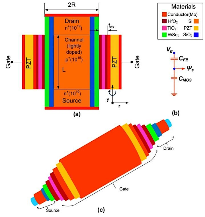
Figure: (a) Cross-sectional view of a cylindrical gate-all-around (GAA) WSe2 NCFET (b) the capacitance model, where the total equivalent capacitance of the 2D FET (CMOS) and FE layer (PZT) capacitance (CFE) are in a series combination and VG acts as the effective gate voltage of the FET including PZT. (c) schematic diagram of GAA WSe2 NCFET
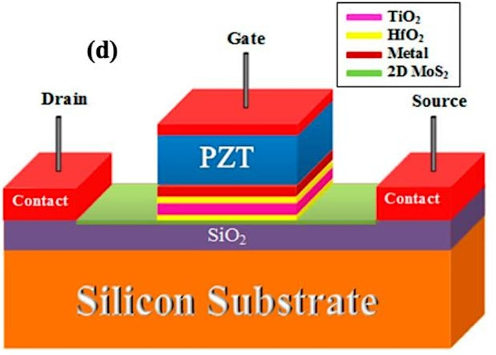
Figure: (d) schematic diagram of the MoS2 negative capacitance FET
The rapid development of the nanoelectronic industry over the past decades has relied on the process of transistor scaling to provide significant improvements to transistor performance at a reduced cost. Multiple directions have been pursued to extend the semiconductor industry’s growing trend, including searching for new material systems, designing new transistor structures, demonstrating new functionalities, and developing new applications.
The semiconductor chip has two main elements: active devices (i.e., transistors) and interconnects.
As for active devices, new 2-D materials (MoS2, WS2, BN, etc.) are all aggressively studied to realize high energy efficiency and memory/logic functions for system compactness. Since the discovery of graphene in 2004, researchers have focused on layer-structured materials and their applications in electron devices.
This talk will present the current status and possible application developments in nanoelectronics and nanomaterials. After a brief introduction, the general nanoelectronics and 2D materials for device applications are discussed. The technical challenges of 2D materials are discussed. This talk will introduce various technologies based on 2D materials and discuss possible applications. In addition, traditional silicon-based devices and nanotechnology-enabled high-performance devices will be discussed.
Read More: Current Prospects and Challenges in Negative-Capacitance Field-Effect Transistors
About the Author:

Dr. Jeongwon Park joined the Department of Electrical and Biomedical Engineering at the University of Nevada, Reno, NV, USA, as an Associate Professor in July 2019.
Prior to that, he was an Associate Professor at the School of Electrical Engineering and Computer Science at the University of Ottawa, Canada (2016-2021, currently Adjunct Professor) and a scientist at SLAC National Accelerator Laboratory, Stanford University, USA (2014 -2016).
For six years (2008-2014), he served as a senior technologist to support the corporate chief technology officer (CTO) and business units at Applied Materials, USA. In addition, he has been a guest researcher at the Lawrence Berkeley National Laboratories (2005-2008), an adjunct professor in the Department of Electrical Engineering at Santa Clara University (2009-2016), and a visiting scholar in the Department of Electrical Engineering at Stanford University, CA, USA (2013-2014).
He received his Ph.D. (2008) in materials science and engineering from the University of California, San Diego, USA. He is a senior member of IEEE and the National Academy of Inventors.
_________________
1:30 — 2:00 PM Optional Covalent Lab Tour – See notes
This tour is open to the public; – however – competitors will not be permitted to tour the lab.
=> If you sign up for the tour – your employer and email information will shared with Covalent Metrology.
=> Signing up for the tour when you register on Eventbrite will not guarantee you a spot on August 22 tour. The number of people that day will be limited.
Overflow – may be accommodated on future tours.
Covalent Metrology is a disruptive analytical services laboratory and digital platform based in Sunnyvale, California. Its mission is to empower technological innovation with superior data and insights. Covalent makes it easier and more affordable to access the metrology data necessary for strategic decision-making: facilitating faster research, development, and production of advanced materials and devices. It is dramatically changing the materials characterization service landscape with the combination of its modern data platform, world-class analysts and top-notch customer service, state-of-the-art analysis instrumentation, and strategic partnerships. Covalent now has over 500 customers in 30+ industries. Learn more at: https://covalentmetrology.com.