IEEE Distinguished Lecture – 75th Anniversary of the Transistor: Evolution, Trends and Challenges in Technology and Device Architectures for Micro- and Nanoelectronics
“75th Anniversary of the Transistor: Evolution, Trends and Challenges in Technology and Device Architectures for Micro- and Nanoelectronics” by Professor Cor Claeys, PhD, Katholieke Universiteit Leuven, Belgium. An IEEE Fellow and IEEE EDS Distinguished Lecturer.
Date: Sept 29, 2023 (Friday)
Time: 10:00 – 12:00 (UTC+8)
Mode: Hybrid
Venue: PSDC, 1 Jalan Sultan Azlan Shah, 11900 Bayan Lepas, Penang, Malaysia
Google Meet: https://meet.google.com/tri-unro-nvk
RSVP: https://forms.gle/S3mH3gAkSLqcxHsS7
All are cordially invited to attend. Admission is FREE. Refreshments will be served from 9:45. Network and interact with like-minded engineers and researchers before the seminar begins. e-Certificates of Attendance will be issued to registered attendees. Pending CPD approval from the Malaysia Board of Technologists.
Abstract
Semiconductor technology has known an exponential evolution in the last decades and is fully integrated in our everyday life. According to the Semiconductor Industry association (SIA) the global semiconductor industry sales reaches about US$ 700 billion in 2023, corresponding with a shipment of more than 1.2 trillion components. This necessitates implementation of novel materials, advanced design concepts and new transistor structures.
Increased device performance and reduced power consumption, while maintaining a good manufacturability and yield performance without penalizing the cost/function, are driving microelectronic research towards 3-nm technologies. A large variety of device architectures such as FinFETs, TFETs, negative capacitance, Gate-All-Around, nanowires (NWs), nanosheets (NSs) in both horizontal or vertical configurations, CFET and Forksheet structures are extensively investigated for both logic and analog/RF building blocks enabling System-on-Chip (SoC) applications. In addition, the huge progress achieved in silicon technology and the heterogenous integration of Ge and III-V technologies on a silicon platform enables the on-chip integration of building blocks with different functionality.
Wide bandgap materials such as GaN offer unique features for RF applications used in base stations for mobile communication, complementing the performance of Si devices suffering from limited output power. These materials can epitaxially be grown on Si substrates. One of the main challenges related to the hetero epitaxy of III-V materials on a Si substrate is the control of extended defects due to the lattice mismatch of the different materials. In recent years, there has been a strong increase in the commercial availability of GaN devices, although for certain applications there is a competition with SiC.
Complex and dense SoC applications can be realized by 3D wafer stacking using Through-Silicon-Vias (TSV) for wafer-to-wafer bonding. The 3D integration results in a reduction of the RC product and interconnect length, a smaller form factor and enables vertical partitioning. Main challenges are the TSV process module itself (e.g. Cu via filling, mechanical stress, contamination, keep-out-zone), the wafer thinning and handling and the 3D stacking technology (stacking density, pitch, chip-to-chip interconnect etc.). Very promising results are obtained for monolithic sequential 3D (S3D) processing based on the processing of different tiers on top of each other. Benefits are related to an enhanced device density per chip area and a shorter interconnection length. A low cost less scalable tier can be processed on top of an expensive scalable tier as done in the case of logic-memory integration.
Major trends in above mentioned process integration approaches are reviewed and technological challenges of some process modules and device structures highlighted.
Speaker
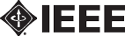
Cor Claeys is Professor at the KU Leuven (Belgium) since 1990. He was with imec, Leuven, Belgium from 1984 till 2016. His main interests are semiconductor technology, device physics, low frequency noise phenomena, radiation effects and defect engineering. He co-edited books on “Low Temperature Electronics” and “Germanium-Based Technologies: From Materials to Devices” and wrote monographs on “Radiation Effects in Advanced Semiconductor Materials and Devices”, “Fundamental and Technological Aspects of Extended Defects in Germanium” and “Random Telegraph Signals in Semiconductor Devices”. Two books are translated in Chinese. He (co)authored 14 book chapters, over 1100 conference presentations and more than 1300 technical papers. He is editor/co-editor of 60 Conference Proceedings. Prof. Claeys is a Fellow of the Electrochemical Society and of IEEE. He was Founder of the IEEE Electron Devices Benelux Chapter, Chair of the IEEE Benelux Section, elected Board of Governors Member and EDS Vice President for Chapters and Regions. He was EDS President in 2008-2009 and Division Director on the IEEE Board of Directors in 2012-2013. He is a recipient of the IEEE Third Millennium Medal and received the IEEE EDS Distinguished Service Award. Within the Electrochemical Society, he was Chair of the Electronics & Photonics Division (2001-2003). In 2004, he received the Electronics & Photonics Division Award. In 2016 he received the Semi China Special Recognition Award for outstanding involvement in the China Semiconductor Technology International Conference (CSTIC).